Recent Post

Saturday, 30 November 2013

3D Printed Abacus iPhone 5s Case

We aren’t sure whether you know how to use the ancient calculating device, but if you just need a unique way to protect your iPhone 5/5s, the 3D printed iPhone 5s case may be suitable for you. This is an interesting form-fitting protective case that measures approx 2.4 x 5.0 x 0.5 inches, and designed for iPhone 5 and iPhone 5s.
3D Printed Abacus iPhone 5s Case

As we can see from the images, the iPhone 5 case is shaped as an abacus along with Apple logo-like beads, and all the tiny beads can be moved smoothly and freely so you can use the protective case as a real abacus. Moreover, the iPhone 5s case is made of white nylon plastic polished to reveal a smooth matte finish in order to protect your iPhone 5/5s from bumps and scratches and provide a comfortable grip. Apart from that, all iPhone buttons and ports are accessible via custom openings.

3D Printed Abacus iPhone 5s Case

The 3D printed abacus iPhone 5s case is priced at $24 USD. If you’re interested, jump to Shapeways official site for more details. Additionally, if you need other options you might like to check O!Coat FaaGaa iPhone 5s case and more via “iPhone 5 case” tag. [Via]
Read more ...

Thursday, 28 November 2013

Room Recorder

My wife was working on a doctoral dissertation and needed to do some field work involving personal interviews in various settings. What would be the best way, technically speaking, to record the interviews? To pass a tape recorder or microphone back and forth seemed too awkward and clipping wired microphones to interviewees didn’t make for a particularly informal atmosphere. Radio microphones seemed overly expensive, too. After some thought, I can up with the "Room Recorder", an add-on microphone preamplifier circuit for use with a tape recorder. While I don’t make any great claim to originality for the circuit, it has produced first class results over one year of interviews and might prove useful to anyone doing similar work.

Circuit diagram:
Room Recorder circuit schematic
Room Recorder Circuit Diagram

The preamplifier was plugged into a Sony Cassette-Corder (any similar device will work) by means of a long, screened microphone cable and placed in a central location in a room or on a bench. The circuit will pick up every whisper, so background noise should be considered when choosing a location. A 2-terminal electret microphone picks up the sound, which is then amplified by a TL071CN low-noise op amp. Note that the microphone’s negative terminal is connected to its case. Negative feedback is applied to the inverting input through a 10kO resistor. Increasing the value of this resistor will increase sensitivity, and vice versa. For ease of use and quietness of operation, the circuit is powered from a 9V battery. The power switch is mounted on the case. The circuit draws about 2mA and would therefore give about 10 days continuous service from a 9V alkaline battery.
Author: Thomas Scarborough - Copyright: Silicon Chip Electronics
Read more ...

Romo the Smartphone Robot

So you happen to be a smartphone user for the past few years already, and have more or less gotten bored of the device, so much so that you are thinking about the possibilities of a new kind of smartphone accessory which would make you a starry-eyed kid once again, with wonder written all over your face.
Romo the Smartphone Robot

Perhaps there might be something out there in the ever evolving consumer market, and the $149.99 Romo the smartphone robot could very well fit your desires to a ‘T’. Romo might even end up being your new best friend if you are a social outcast, as Romo will learn and grow up with you the more time you spend with it and interact alongside. Basically, I guess you could call this the geek’s Furby, as the more you make use of him, the faster and more he will be able to learn.

Sure, he looks cute as heck – at least getting near Wall-E levels, and is controllable via any Wi-Fi enabled computer or iOS device. The Romo the smartphone robot might be the perfect fodder to help you break down walls if you are not too good with kids, and it also brings your standard video chat sessions to a totally new level. [Via]
Read more ...

Tuesday, 26 November 2013

Power Diode For Solar Power Systems

Apart from the sun, solar power systems cannot work without a reflow protection diode between the solar panel and the energy store. When current flows into the store, there is a potential drop across the diode which must be written off as a loss in energy. In the case of a Schottky diode, this is not less than 0.28 V at nominal current levels, but will rise with higher ones. It is clear that it is advantageous to keep the energy loss as small as possible and this may be achieved with external circuitry as shown in the diagram. The circuit is essentially an electronic switch consisting of a high precision operational amplifier, IC1a, a Type OP295 from Analog Devices, and a MOSFET, T1.

This arrangement has the advantages over a Schottky diode that it has a lower threshold voltage and the lost energy is not dissipated as heat so that only a small heat sink is needed. When the potential at the non-inverting input of the op amp, which is configured as a comparator, rises above that at the inverting input, the output switches to the operating voltage. The transistor then comes on, whereupon light-emitting diode LD1 lights. Diode D3 clamps the inputs of IC1a so that the peak input voltage cannot be greater than half the threshold voltage, provided the values of R3 and R4 are equal.

Power Diode For Solar Power Systems
The op amp provides very high small-signal amplification, a small offset voltage, and consequent fast switching. The MOSFET changes from on to off state and vice versa at drain -source voltages in the microvolt range. In the quiescent state, when UDS is 0 V, the transistor is on, so that LD1 lights. The operating voltage (C–A) may be between 5 V (the minimum supply for the op amp and the input control potential, UGS, of the transistor) and 36 V (twice the zener voltage of D1). Zener diode D1 protects the MOSFET against excessive voltages (greater than ±20 V). Diode D3 and resistors R3 and R4 halve the potential across the inputs of the op amp.

This ensures that operation with reversed or open terminals is harmless. The substrate diode of the MOSFET is of no consequence since it does not become forward biased as long as the forward voltage, USD, of the transistor is held very low. The on -resistance, RSD(on), of the transistor is only 8 mΩ and the transistor can handle currents of up to 75 A. When the nominal current is 10 A, the drop across the on-resistance is 80 mV, resulting in an energy loss of 0.8W. This is low enough for a SUB type with a TO263-SMD case to be used without heat sink. When the current is 50 A, however, it is advisable to use a SUP type with a TO220 case and a heat sink since the transistor is then dissipating 12.5 W.

Even then, the voltage drop, USD = 0.32 V is significantly lower than that across a Schottky diode in the same circumstances. Moreover, owing to the high precision of IC1a, a number of transistors may be used in parallel. The circuit proper draws a current of 150 µA when only one of the op amps in the OP295 is used. An even lower current is drawn by the alternative Type MAX478 from Maxim. However, the differences between these two types are only relevant in the low current and voltage ranges. Both have rail-to-rail outputs that set the control voltage accurately even at very low operating voltages.

This is important since the switch-on resistance of MOSFETs is not constant: t drops significantly with increasing gate potentials and decreasing temperature. A experimental circuit may use an LM358 op amp and a Type BUZ10 transistors, but these components do not give the excellent results just described.
Read more ...

Saturday, 23 November 2013

Toshiba Excite 7 Android Tablet Announced

Toshiba has announced Excite 7, its latest Android tablet. If you’re looking for a balance option between price and performance, the 7-inch tablet may be able to catch your eyes. Toshiba Excite 7 is a budget friendly and high performance Android tablet that runs on Google Android 4.2.2 Jelly Bean mobile operating system.
Toshiba Excite 7 Android Tablet Announced

The Android tablet is powered by Rockchip RK3188 quad-core processor, and comes with 1GB RAM, 8GB eMMC internal storage, 7-inch capacitive 5-finger multi-touchscreen LCD display with 1024 x 600 pixels resolution, 0.3-megapixel front-facing webcam and 3-megapixel rear camera.

Moreover, other specs also include WiFi, Bluetooth 4.0, microSD card slot, stereo speakers and 14W-hours rechargeable battery for up to 8 hours of video playback. Toshiba Excite 7 Android tablet is priced at $169.99 USD. If you’re interested, jump to Toshiba official site for more details.
Read more ...

Thursday, 21 November 2013

Flashback iPhone 5s Case

Hard-shell iPhone5 case in a throwback design that'll have you partying like it's the year 2000. Allows for full access to all ports and controls & easily snaps right on n' off.
Flashback iPhone 55s Case

Content care ,Plastic,Wipe clean,Imported,Size Fits iPhone 5

Flashback iPhone 55s Case

Read more ...

Cookie Shaped USB Mug Warmer

Want to comfortably enjoy your favorite coffee beside your computer? Take a look at the cookie shaped USB mug warmer, it may be able to catch your eyes. This is an interesting and practical USB mug warmer that measures 4 inches in length and 1 inch in width.
Cookie Shaped USB Mug Warmer

As we can see from the images, the USB mug warmer is shaped as a chocolate sandwich cookie, and features delicious details and colors. Of course, you can put it into your mouths, but using integrated USB cable you can connect the cookie shaped USB cup warmer to your computer in order to keep your favorite beverage piping hot – up to 140 degrees. Apart from that, the mug warmer is compatible with all Mac and PCs.
Cookie Shaped USB Mug Warmer
The cookie shaped USB mug warmer is priced at $14 USD. If you’re interested, jump to Urban Outfitters for more details.
Read more ...

Wednesday, 20 November 2013

Timebrick Concrete Clock

It’s not a normal concrete block, but a unique clock that shows you accurate time. If you like this kind of solid design, let’s go on checking the Timebrick concrete clock. The Timebrick is a pretty cool desktop timepiece that measures 8.5 x 8.5 x 5.3cm and weights 486g.
Timebrick Concrete Clock

As we can see from the images, the desktop clock features low-profile and stylish design, most importantly, the timepiece comes with a unique casing made from concrete along with bold accents including hexagonal screws and squat hands for extremely durable construction and personalized design.

Inside, there is a German Quartz UTS movement in order to show you accurate time, moreover, the concrete clock is powered by an AA battery. The Timebrick concrete clock is available in 6 colors, each one is priced at $49 USD. If you’re interested, jump to TouchOfModren online store for more details. [Via]
Read more ...

Tuesday, 19 November 2013

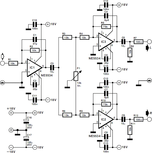
Pan Pot

A pan pot enables a mono-phonic input signal to be positioned where desired between the stereo loudspeakers. When P1 (see diagram) is in the center position, there is no attenuation or amplification between the input and output. When the control is turned away from the center position, the signal in one channel will be amplified 3 dB more than the other. Circuit IC1 at the input is a buffer stage.

It is arranged as an inverter to ensure that the phase of the input signal is identical to that of the output signal. The input impedance is set by R1 (10 kΩ). The output of the buffer is applied to stereo amplifiers IC2 and IC3. A special arrangement here is the positioning of P1, in conjunction with R3, R4, R8, and R9, in the feedback circuits of both amplifiers. This means that any adjustment of the potentiometer will have opposite effects in the amplifiers.
Pan Pot

Series resistors R7 and R12 serve to ensure that the outputs can handle capacitive loads. Coupling capacitors C3, C6, and C9, may be omitted if an offset voltage of 20–30 mV is of no consequence in the relevant application. Capacitors C2, C5, and C8, ensure that the op amps remain stable even at unity gain. Capacitors C1, C4, and C7, minimize any r.f. interference, resulting in a usable bandwidth of 2.5 Hz to 200 kHz.

The performance of the circuit is of sufficiently high quality to allow the pot being incorporated in good-quality control panels. Total harmonic distortion plus noise (THD+N) at a frequency of 1 kHz and a bandwidth of 22 kHz is 0.0014%. Over the band 20 Hz to 20 kHz and a bandwidth of 80 dB, this figure is still only 0.0023%. The circuit needs a power supply of ±18 V, from which it draws a current of about 16 mA.
Read more ...

Monday, 18 November 2013

Sounds From The Old West

This circuit shows how far integration can be taken: IC1, a Type HT82207 from Holtek does virtually everything. Only a (small) loudspeaker and the necessary selectors need to be added. The standard 18-pin Type HT82207 is an integrated sound generator, producing sounds typical of the Old West. The various sounds are selected by S1–S6 as listed below. In the quiescent state, the circuit draws a current not exceeding 1 µA.
  • S1 – bugle
  • S2 – neighing
  • S3 – sound of hooves
  • S4 – pistol shot
  • S5 – crack of a rifle
  • S6 – cannon fire

Read more ...

Modem Off Indicator

The modem off indicator is intended especially for serious Internet surfers. It will be seen that the circuit of the indicator cannot be much simpler, or there might be nothing left. In spite of its simplicity, it may prove to be a cost-saving device, since it shows at a glance whether the telephone line is free again after the modem has been used. This obviates high telephone charges in case for some reason the modem continues to operate. The circuit depends on the fact that there is a potential of about 40 V on the telephone line when it is not busy. This voltage drops sharply when a telephone call is being made. If, therefore, the circuit is linked to telephone terminals a and b, the lighting of the green LED shows that the line is not busy in error.
Modem Off Indicator


The bridge rectifier ensures that the polarity of the line voltage is of no consequence. This has the additional benefit that polarity protection for the LED is not necessary. To make sure that the telephone line is not loaded unnecessarily, the LED is a high efficiency type. This type lights at a current as low as 2 mA, and this is, therefore the current arranged through it by resistor R1.

WARNING.
In spite of the liberal age we live in, it is highly probable that in many countries it is not allowed to connect the indicator across the telephone lines. Seek advice of your local telephone company that owns or operates the telephone network.
Read more ...

Oscillation Monitor

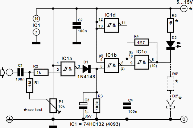
The circuit in the diagram was originally designed to monitor an oscillator, but can also be used as a general-purpose level indicator for a.c. signals. It is based on a quadruple IC containing four NAND gates. Only three of the gates are used, making the fourth free for other purposes. All the gates have a Schmitt trigger input.

When a 5 V supply is used, the Type 74HC132 is recommended; for higher voltage, a Type 4093. Note, however, that these two ICs have different pinouts. In the diagram, the differing pins of a 4093 are shown in brackets. The signal to be monitored is applied to the input of the first gate via capacitor C1. Resistor R2, in conjunction with the protection diode in the IC, guards the input to high voltages.

In the absence of a signal, resistor R1 holds the input high so that the output of the gate is low. When a signal of sufficient strength is received, the input of the gate goes low during the negative half cycle of the signal, so that the output of the gate goes high in rhythm with the input signal. However, the Schmitt trigger converts sinusoidal signals into rectangular ones, which charge capacitor C3 via diode D1. When the potential across C3 exceeds the threshold at the input of the second gate, this gate also toggles. The output of the second gate is then low, which disables the third gate, which functions as an oscillator. When the level of the input signal drops, C3 is discharged via R3.
Oscillation Monitor

The potential across the capacitor then no longer exceeds the threshold at the input of IC1b, whereupon IC1c is enabled and the LED flashes The LED may be connected as shown or as indicated by the dashed line. As shown, the diode remains off when there is an input signal of sufficient strength and begins to flash when the signal fails or its level drops. When the diode is linked to earth, it is on continuously when there is an input signal, and begins to flash when the input drops. When a 5 V power supply is used, R5 = 1 kΩ, and the circuit draws a current, including that of the LED, of 3 mA. The frequency of the input signal may lie between 10 Hz and 10 MHz. When a 9–12 V supply is used, the value of R5 must be altered as necessary.

Owing to the 4093 being slower than the 74HC132, the upper frequency of the input signal is then limited to 3 MHz. When the wiper of P1 is at the level of the supply voltage, the response threshold, USS, lies between 3.5 V (when Ub =5V) and 7 V (when Ub =12V). When the wiper is moved away from the positive supply line, USS (max) is 1.5 V (when Ub = 5 V). The response threshold is quite precise: a drop in the input signal level of 50–100 mV is sufficient to disable the input. When the input level is too high, a preset across the input terminals enables the level to be reduced to a value that lies in the desired range above the response threshold.
Read more ...

Opamp With Hysteresis

At first glance, the circuit in the diagram does not look out of the ordinary, and yet, it is. This is because it combines two characteristics that are usually assumed to be incompatible: hysteresis and a high input impedance. In a standard op amp circuit, this is, indeed, true, because the creation of hysteresis is normally achieved by positive feedback to the +ve input of the op amp. Unfortunately, the requisite resistance network causes a drastic deterioration of the original high input impedance of the op amp. So, when a high input impedance and hysteresis are wanted, the solution is to obtain the needed positive feedback by coupling the resistor network not to the +ve input but to the offset correction pin.
Opamp With Hysteresis

When this done, the hysteresis so obtained is calculated from Uh = 1.2/R4Uo, where Uh is the hysteresis voltage and Uo is the output voltage of the op amp, both in volts The value of R4 must be in kΩ. The level of Uo depends, of course, on the load.
Read more ...

Sunday, 17 November 2013

Low-Power Voltage Reference

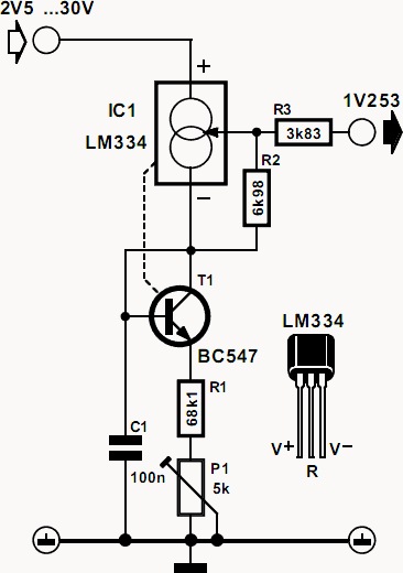
The present reference is a special application of current source IC Type LM334. It has a tiny temperature coefficient and draws only a minute current: at room temperature, only 10 µA, which increases with large rises in temperature by only a few µA. The circuit is basically a bandgap reference, because the positive temperature coefficient of the LM334 is combined with the negative temperature coefficient of the base-emitter junction of a transistor (which ensures good thermal coupling).

To obtain a temperature coefficient of zero, or very nearly so, the output voltage of the circuit is adjusted to exactly 1.253 V with P1. It is, therefore, advisable to measure the set value of P1 accurately after it has been adjusted and to replace the combination of R1+P1 by a fixed resistor of the precise value.
Low-Power Voltage Reference

Use a 1% metal-oxide film type from the E96 series. Since current source IC1 is tapped at the control input, a reference source with a negative output resistance of about 3.8 kΩ ensues. Resistor R3 ensures that the ultimate output resistance is about 400 Ω. The load current is then limited to not more than 5 µA. The performance of the reference is good: when the input voltage is increased from 5 V to 30 V, the output voltage varies by only 0.6 µV (from 1,2530 V to 1.2536 V). The temperature coefficient stays below 50 ppm °C–1, and, with careful adjustment, may even come down to 5 ppm °C–1. The current drawn by the prototype is 9.8 µA at an ambient temperature of 22 °C.
Read more ...

Mini Audio Signal Generator

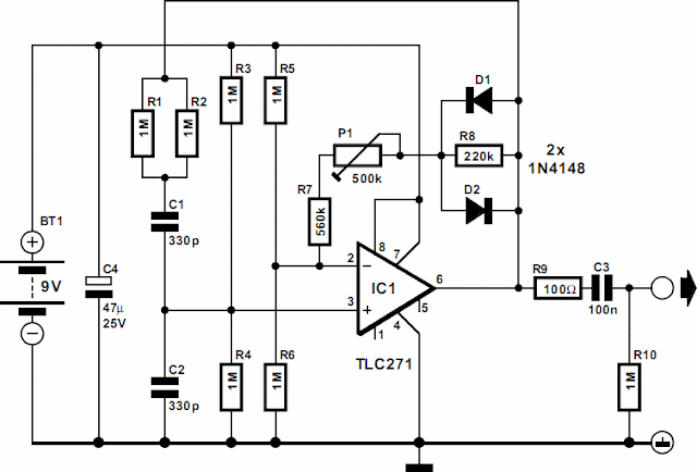
A small audio test generator is very useful for quickly tracing a signal through an audio unit. Its main purpose is speed rather than refinement. A single sine-wave signal of about 1 kHz is normally all that is needed: distortion is not terribly important. It is, however, important that the unit does not draw too high a current. The generator described meets these modest requirements.

It uses standard components, produces a signal of 899 Hz at an output level of 1 V r.m.s. and draws a current of only 20 µA. In theory, the low current drain would give a 9 V battery a life of 25,000 hours. The circuit is a traditional Wien bridge oscillator based on a Type TLC271 op amp. The frequency determining bridge is formed by C1, C2 and R1–R4. The two inputs of the op amp are held at half the supply voltage by dividers R3-R4 and R5-R6 respectively.
Mini Audio Signal Generator

Resistors R5 and R6 also form part of the feedback loop. The amplification is set to about ´3 with P1. Diodes D1 and D2 are peak limiters. Since the limiting is based on the non-linearity of the diodes, there is a certain amount of distortion. At the nominal output voltage of 1 V r.m.s., the distortion is about 10%. This is, however, of no consequence in fast tests.

Nevertheless, if 10% is considered too high, it may be improved appreciably by linking pin 8 of IC1 to ground. This increases the current drain of the circuit to 640 µA, but the distortion is down to 0.7%, provided the circuit is adjusted properly. If a distortion meter or similar is not available, simply adjust the output to 1 V r.m.s. Since the distortion of the unit is not measured in hundredths of a per cent, C1 and C2 may be ceramic types without much detriment.
Read more ...

Active Short-Wave Antenna

The circuit presented here illustrates the fact that in spite of all kinds of new component and technology, it is still possible to design useful, and interesting, circuits. The circuit is based on two well-established transistors, a Type BF256C and a BF494. In conjunction with the requisite resistors and capacitors, these form a well-working antenna amplifier. Note that they are direct coupled. Transistor T1 is the input amplifier cum buffer, while the BF494, in a common-ground configuration, provides the necessary amplification. The amplifier is designed for operation at frequencies between 10 MHz and 30 MHz, which is the larger part of the short-wave range, and has a gain of 20 dB.
Active Short-Wave Antenna

Inductor L1 is wound on an Amidon core Type T-37-6. The primary consists of 2 turns, and the secondary of 12 turns 0.3 mm dia. enameled copper wire. The number of turns may be experimented with for other frequency ranges. The input circuit is tuned to the wanted station with capacitor C1. The response of the tuned circuit is fairly broad, so that correct tuning is easy. The circuit is powered by a well-decoupled mains supply converter that has an output of 9–12 V. The circuit draws a current of about 5mA.
Author: G. Pradeep
Copyright: Elektor Electronics
Read more ...

Saturday, 16 November 2013

Rear Light After Glow (For Bicycles)

This article is of interest only to readers whose bicycle lights are powered by a dynamo. The laws on bicycle lights in the United Kingdom are stricter than in other countries and a dynamo is, therefore, a rarity in this country. From the point of view of traffic safety it is advisable (in UK obligatory) for cyclists to have the rear lamp of their bicycle to light even when they are at standstill. In principle, it is not very difficult to modify the existing rear light with afterglow: all this needs is a large enough energy reservoir. Since the after-glow is required for short periods of time only, a battery is not required: a large value capacitor, say, 1 F, is quite sufficient.

As the diagram shows, in the present circuit, the normal rear light bulb is replaced by two series-connected bright LEDs, D2 and D3. These are clearly visible with a current of only 6 mA (compared with 50 mA of the bulb). The current is set with series resistor R1. The LEDs are shunted by the 1 F capacitor, C1. Since the working voltage of this component is only 5.5 V, it is, in spite of its high value, physically small. An effective regulator is needed to limit the dynamo voltage adequately. Normal regulators cannot be used here, since they do not work at low voltages. Moreover, such a device would discharge the capacitor when the cycle is at standstill.
Rear Light After Glow (For Bicycles)

Fortunately, there is a low-drop type that meets the present requirements nicely: the Type LP2950CZ5.0. Of course, the dynamo output voltage needs to be rectified before it can be applied to the regulator. In the present circuit, this is effected by half-wave rectifier D1 and buffer capacitor C2. Diode D1 is a Schottky type to keep any losses low – important for this application, because the ground connection via the bicycle frame usually causes some losses as well. The value of buffer capacitor has been chosen well above requirements to ensure that C1 is charged during the negative half cycles of the dynamo voltage.
Read more ...

Saturday, 9 November 2013

Digital Main Voltage Indicator

Continuous monitoring of the mains voltage is required in many applications such as manual voltage stabilisers and motor pumps. An analogue voltmeter, though cheap, has many disadvantages as it has moving parts and is sensitive to vibrations. The solidstate voltmeter circuit described here indicates the mains voltage with a resolution that is comparable to that of a general-purpose analogue voltmeter. The status of the mains voltage is available in the form of an LED bar graph. Presets VR1 through VR16 are used to set the DC voltages corresponding to the 16 voltage levels over the 50-250V range as marked on LED1 through LED16, respectively, in the figure. The LED bar graph is multiplexed from the bottom to the top with the help of ICs CD4067B (16-channel multiplexer) and CD4029B (counter).

The counter clocked by NE555 timer-based astable multivibrator generates 4-bit binary address for multiplexer-demultiplexer pair of CD4067B and CD4514B. The voltage from the wipers of presets are multiplexed by CD4067B and the output from pin 1 of CD4067B is fed to the non-inverting input of comparator A2 (half of op-amp LM358) after being buffered by A1 (the other half of IC2). The unregulated voltage sensed from rectifier output is fed to the inverting input of comparator A2. The output of comparator A2 is low until the sensed voltage is greater than the reference input applied at the non-inverting pins of comparator A2 via buffer A1.
Digital Main Voltage Indicator

When the sensed voltage goes below the reference voltage, the output of comparator A2 goes high. The high output from comparator A2 inhibits the decoder (CD4514) that is used to decode the output of IC4029 and drive the LEDs. This ensures that the LEDs of the bar graph are ‘on’ up to the sensed voltage-level proportional to the mains voltage.The initial adjustment of each of the presets can be done by feeding a known AC voltage through an auto-transformer and then adjusting the corresponding preset to ensure that only those LEDs that are up to the applied voltage glow.

Note.
It is advisable to use additional transformer, rectifier, filter, and regulator arrangements for obtaining a regulated supply for the functioning of the circuit so that performance of the circuit is not affected even when the mains voltage falls as low as 50V or goes as high as 280V. During Lab testing regulated 12-volt supply for circuit operation was used.)
Read more ...

Turtle Beach Anounces iSeries Media Headsets.

When it comes to audio brands, there is one particular name that stands out above the rest for some people, and Turtle Beach would be one of them. The name Turtle Beach has long been synonymous with high quality audio devices, and this time around the company has announced their spanking new iSeries range of high end media headsets.

The iSeries will arrive in the form of the wireless surround sound i60 and the wireless amplified stereo i30, where these would no doubt be the first headsets that have been specially constructed for use with both Mac and iOS products. The iSeries headsets themselves will arrive with a bunch of innovations that Turtle Beach originally introduced to gaming headsets but so happen to be new for mobile users. Hopefully, with a little bit of something for everyone, folks will be satisfied.

Some of the new features introduced to gaming headsets that mobile users would fall in love with include improved chat and voice call quality as well as an unmatched level of control over audio. Regardless of whether you settle for the i60 or the i30, they will both share the same unique design which blends style, quality, comfort and durability, while boasting premium finishes, where among them include a leather headband and leather-covered memory foam, noise-isolating ear cups.
Turtle Beach Anounces iSeries Media Headsets.
The two headsets will also be accompanied by a built-in remote which plays nice with the iPhone, iPad and the Mac. They will come with innovative dual boom-less microphones which will hopefully, deliver clear, high-quality audio during chat, voice calling and use with Siri.

Of course, the i60 will be the flagship model, where it features a control unit for use with Mac desktops and laptops that deliver fingertip audio and preset control. Turtle Beach does have some pretty high hopes that the i60 will also be the first wireless headset for the Mac platform that boasts of 7.1 DTS surround sound with adjustable speaker angles and EQ presets, a fully programmable digital signal processor (DSP), dual-band Wi-Fi for uncompressed, interference free wireless audio and dual-pairing Bluetooth 4.0 connectivity. [Via]
Read more ...

Wednesday, 6 November 2013

Bike Battery Charger

This simple circuit allows a 12V battery pack to be charged via a bike generator. The generator is rated at 3W and with this voltage multiplier circuit provides about 200mA at about 15km/h. A 12V system was chosen because it allows the use of a car horn (get noticed)! Two 6V 3W globes in series provides adequate lighting and they last more than six months

Circuit diagram:
Bike battery charger circuit schematic
Bike Battery Charger Circuit Diagram
Author: Paul Breuker
Copyright: Siicon Chip Electronics
Read more ...

Monday, 4 November 2013

Google Nexus 5 Android Phone Now Available

Google Nexus 5 has been available at Google Play, including two memory models and two colors. If you’re curious, let’s go on checking the official Android phone. Google Nexus 5 is a high performance Android smartphone that measures 69.17 x 137.84 x 8.59mm and weights 130g.

Google Nexus 5 Android Phone Now Available
The smartphone runs Google’s latest Android 4.4 KitKat mobile operating system, and as we can see from the images, Nexus 5 also features sleek ultra-slim design, and comes with a Qualcomm Snapdragon 800 2.26GHz quad-core processor with Adreno 330 450MHz GPU, 2GB RAM, 16GB/32GB internal storage, 4.95-inch full HD IPS display with 1920 x 1080 pixels resolution and Corning Gorilla Glass 3, 1.3-megapixel front-facing camera, and 8-megapixel rear camera with optical image stabilization. Moreover, Nexus 5 also has Bluetooth 4.0, NFC, dual-band WiFi, GPS, built-in wireless charging as well 2300mAh rechargeable battery that offers 17 hours of talk time.

Google Nexus 5 Android smartphone comes in two colors and two memory version, and starting at $349 USD. If you’re interested, jump to Google official site for more details.
Read more ...

Low-Voltage Cutout For 12V SLA Batteries

This simple circuit protects an SLA battery from over-discharge by disconnecting the load when the terminal voltage drops below a preset level. In operation, a sample of the battery voltage is derived from the 22kΩ resistor and 20kΩ trimpot divider. This is applied to the non-inverting input (pin 3) of IC1, where it is compared with a reference voltage on the inverting input (pin 2). When the sampled battery voltage falls below the reference voltage, IC1’s output (pin 1) swings towards ground, switching Mosfet Q2 off and disconnecting the load from the battery. The reference voltage is derived from a 4.7V zener diode (ZD1), which is connected to ground via the collector-emitter circuit of Q1 (ie, when Q1 is on).

Circuit diagram:
Low-voltage cutout for 12V SLA batteries circuit schematic

However, when the op amp’s output is driven low, Q1 is switched off, causing the non-inverting input to rise towards the full battery voltage. This greatly reinforces the switching action, latching the circuit in the "off" state until the battery is recharged and the reset switch (S1) pressed. The Mosfet used for Q2 should be selected to suit the intended application. The circuit could also drive a relay simply by connecting the coil across the "load" terminals. As is usual practice, a diode should be connected across the relay coil to limit back-EMF spikes.
Author: Tim Nuske - Copyright: Silicon Chip Electronics
Read more ...

Video Games and Computer Performance

If you’re an avid computer game player, you’ve probably run across one that slows down your computer. You’ll notice it’s a little more difficult to run other programs when you have a game running, and the game itself might get choppy or even shut down. There are a few different reasons this could happen, but here’s some basic information behind why your computer doesn’t always run as well when playing a video game.
Computer Hardware

Your computer has a limited number of resources it can dedicate to a task. When one task takes up resources, it can’t dedicate as much to others. A task that requires a huge amount of resources, like a graphics-intensive video game, may overburden your computer’s hardware. Although there are many programs that don’t take much computing power to run, a lot of small programs running at the same time can have the same impact as one big resource hog.

What Do These System Requirements Mean, Anyway?

Most computer games come with a list of system requirements. Your computer has a lot of components, but there are a few big ones that impact your computer’s ability to play a video game.
Processor Speed

Think of your computer’s processor like a band conductor. The conductor uses gestures to give instructions so that the entire band can play in unison. A really good conductor can give these instructions with exceptional speed. The processor is responsible for telling the rest of your computer what to do. The faster your processor, the faster it can give out these instructions.
Hard Drive

Your computer’s hard drive is like a digital filing cabinet. It stores all the files and programs your computer needs to run and everything else you download and install. A full

hard drive will also make your computer run slowly, so you’ll want to leave some free space.

Random Access Memory (RAM)

RAM – frequently referred to as “memory” – is kind of like your computer’s short-term memory. RAM stores data for your computer’s processor to access, but will only store it as long as your computer is running. Accessing data from RAM is faster than accessing it from your hard drive, which is why having more RAM may make programs run faster. Your computer does have limits on how much RAM it can support, so don’t go on too big of a RAM-purchasing spree.

The video card is designed specifically to create images out of digital information. New video cards have their own processor and memory, so they can create images rapidly without adding more burden to your computer’s regular processor.

How to Improve Performance:

There are actually a few things you can do yourself that will improve how well your computer runs, especially when playing computer games.

Since every program running on your computer takes up some resources, close the ones you don’t need when you’re playing a game. Browsers, movies and even instant messengers can impact how well your computer performs! Scan for and remove viruses on a regular basis. Viruses, spyware and adware are all programs, and they use your computer’s resources to spread themselves around!

If your hard drive is getting a little full, it may be time to do some digital spring cleaning. Uninstall programs you no longer use, empty the recycle bin and delete movies you don’t plan on watching again. Avoid deleting something if you don’t know what it is, or you may accidentally get rid of something your computer needs.

You might also want to defragment your hard drive. Windows has a built-in defragmentation tool that you can use, and there are third-party programs available to defragment Mac systems.
Read more ...

10 Awesome Computer Tips Everyone Should Know

Here are some useful tricks to help you be a more efficient and knowledgeable computer user:

  1.     Windows+L: Locks your computer
  2.     Windows+P: Quickly sets up a second screen and/or monitor
  3.     Windows+D: Minimize all open windows
  4.     Windows+Tab: Switch windows
  5.     Control+F: Opens a search box where you can search through text on a web page or document
  6.     Control+Enter: Wraps whatever you type into a browser with the “http://www”  before and “.com”  after it
  7.     Control+Shift+N: Opens up incognito mode in Google Chrome
  8.     Click on your mouse wheel to open a link in a new tab
  9.     When you install something, watch what you’re doing instead of just NEXT, NEXT, NEXT through everything. A lot of programs will install annoying toolbars by default, which take up space on your screen and are difficult to remove.
  10.     Utilize programs such as CCleaner  and Defraggler to keep your computer running in optimal condition.

Read more ...

Saturday, 2 November 2013

Android SDK Installation Guide

Here’s a quick start installation guide to get you up and running with the Google Android Software Development Kit (SDK). This guide will describe how to install the Android SDK and set up your chosen development environments. If you’ haven’t already done so you can download the Android SDK from the link below, then we can get started.

First you’ll need to download the Android SDK source files:
  http://code.google.com/android/download.html  


System Requirements

In order to first use the Android SDK code and tools for development you will of course need a suitable environment develop from.

Currently the following operating systems are supported:

    Windows XP or Vista
    Mac OS X 10.4.8 or later (x86 only)
    Linux (tested on Linux Ubuntu Dapper Drake)

You will also need to install a suitable development environment such as:

Eclipse
    Eclipse 3.2, 3.3 (Europa)
    Android Development Tools plugin (optional)

    Other development environments or IDEs

    JDK 5 or JDK 6 (JRE alone is not sufficient)
    Not compatible with Gnu Compiler for Java (gcj)
    Apache Ant 1.6.5 or later for Linux and Mac, 1.7 or later for Windows

Installing The Android SDK


First you will need to download the Android SDK pack .zip archive, once downloaded find a suitable installation location on your machine and extract the zipped files.

Please note: This installation location will be referred to as $SDK_ROOT from now on through this tutorial

Alternatively you can add /tools to your root path which will prevent the need to specify the full path to the tools directory along with enabling you to run Android Debug Bridge (adb) along with other command line tools.

To add /tools:

Linux
  1.     Edit the ~/.bash_profile or ~/.bashrc files looking for a line that sets the PATH variable.
  2.     Add the full path location to your $SDK_ROOT/tools location for the PATH variable.
  3.     If no PATH line exists you can add the line by typing the following:
  4.     export PATH=${PATH}:

Mac OS X

  1.     In the home directory locate the .bash_profile and locating the PATH variable add the location to your $SDK_ROOT/tools folder.

Windows XP / Vista
  1.     Right click on the My Computer icon and select the properties tab.
  2.     Select the Advanced tab and click the Environment Variables button.
  3.     In the new dialog box dowble-click on Path (located under System Variables) and type in the full path location to the tools directory.

The Android SDK also requires a suitable development environment to work in, here’s the installation guides for each of the supported environments.

Android Eclipse Plugin (ADT)

If you choose to use the Eclipse IDE as your Android development environment you will have the opportunity to install and run a plug-in called Android Development Tools. ADT comes with a variety of powerful tools and extensions that will make creating, running and debugging your Android applications much easier and faster.

In order to download and install ADT you will first need to configure an Eclipse remote update, this can achieved via the following steps:
  1.     Start Eclipse, then select Help > Software Updates > Find and Install….
  2.     In the dialog that appears, select Search for new features to install and press Next.
  3.     Press New Remote Site.
  4.     In the resulting dialog box, enter a name for the remote site (e.g. Android Plugin) and enter this as its URL: https://dl-ssl.google.com/android/eclipse/.
  5.     Press OK.
  6.     You should now see the new site added to the search list (and checked).
  7.     Press Finish.
  8.     In the subsequent Search Results dialog box, select the checkbox for Android Plugin > Eclipse Integration > Android Development Tools and press Next.
  9.     Read the license agreement and then select Accept terms of the license agreement, if appropriate.
  10.     Press Next.
  11.     Press Finish.
  12.     The ADT plugin is not signed; you can accept the installation anyway by pressing Install All.
  13.     Restart Eclipse.
  14.     After restart, update your Eclipse preferences to point to the SDK root directory ($SDK_ROOT):
  15.     Select Window > Preferences… to open the Preferences panel. (Mac OS X: Eclipse > Preferences)
  16.     Select Android from the left panel.
  17.     For the SDK Location in the main panel, press Browse... and find the SDK root directory.
  18.     Press Apply, then OK

Updating the ADT Plugin


To update the ADT plugin to the latest version, follow these steps:
  1.     Select Help > Software Updates > Find and Install….
  2.     Select Search for updates of the currently installed features and press Finish.
  3.     If any update for ADT is available, select and install.

Alternatively:
  1.     Select Help > Software Updates > Manage Configuration.
  2.     Navigate down the tree and select Android Development Tools
  3.     Select Scan for Updates under Available Tasks.

How-To Use Eclipse To Develop Android Applications


In order to begin development on your Android applications you will first need to create a new Android project and then configure a launch configuration. Once completed you will have the capability to write, run and debug your Android creations.

The following sections below will provide you with the necessary instructions to get you up and running with Android provided you have installed the ADT plugin (as previously mentioned) in your Eclipse environment.
Creating A New Android Project

The Android Development Tools plugins kindly provides a Wizard for setting up new Projects which will allow us to create new Eclipse projects relatively quickly for either new or existing code.

Select File > New > Project

    Select Android > Android Project, and press Next
    Select the contents for the project:

    Select Create new project in workspace to start a project for new code. Enter the project name, the base package name, the name of a single Activity class to create as a stub .java file, and a name to use for your application.
    Select Create project from existing source to start a project from existing code. Use this option if you want to build and run any of the sample applications included with the SDK. The sample applications are located in the samples/ directory in the SDK. Browse to the directory containing the existing source code and click OK. If the directory contains a valid Android manifest file, the ADT plugin fills in the package, activity, and application names for you.

Press Finish.

Once completed the ADT plugin will go ahead and create the following files and folders as appropriate for the type of project selected:

    src/ A folder that includes your stub .java Activity file.
    res/ A folder for your resources.
    AndroidManifest.xml The manifest for your project.

Creating A Launch Configuration For Eclipse


In order to be able to run and debug your own Eclipse applications you must first create a launch configuration. Simply, a launch config is used to specify which project to launch, which activity to start and the specific emulation options to use.

To create a launch configuration for the application, please see the following steps:
1. Select Run > Open Run Dialog… or Run > Open Debug Dialog… as appropriate.
2. In the project type list on the left, right-click Android Application and select New.
3. Enter a name for your configuration.
4. On the Android tab, browse for the project and Activity to start.
5. On the Emulator tab, set the desired screen and network properties, as well as any other emulator startup options.
6. You can set additional options on the Common tab as desired.
7. Press Apply to save the launch configuration, or press Run or Debug (as appropriate).
Running and Debugging an Eclipse Application

Once both steps 1 and 2 have been completed and your project and launch configs are up and running you will now be able to run or debug your application.

From the Eclipse main menu, select Run > Run or Run > Debug as appropriate. This command will run or debug the most recently selected application.

To set or change the active launch configuration, use the Run configuration manager, which you can access through Run > Open Run Dialog… or Run > Open Debug Dialog….

Running or debugging the application will trigger the following actions:


  1.     Starts the emulator, if it is not already running.
  2.     Compile the project, if there have been changes since the last build, and installs the application on the emulator.
  3.     Run starts the application.
  4.     Debug starts the application in “Wait for debugger” mode, then opens the Debug perspective and attaches the Eclipse Java debugger to the application.

Developing Android Applications with Other IDEs and Tools


Although it is recommended you use Eclipse with the Android plugin to develop your applications, the SDK also provides tools which will enable you to develop with other IDE’s including intelliJ (alternatively you could just use Eclipse without the plugin).
Creating an Android Project

Bundled with the Android SDK is a program called activityCreatory. activityCreator will generate a number of ‘stub’ files for your chosen project alongside a build file. This can be used to either create an Android project for new code or from existing code.

For Linux and Mac users the Android SDK provides a Python script called activityCreator.py, with Windows users receiving a btach script called activityCreator.bat. The program is used in the same way regardless of operating system.

In order to run activityCreator and create an Android project, follow these steps:


    In the command line, change to the tools/ directory of the SDK and create a new directory for your project files. If you are creating a project from existing code, change to the root folder of your application instead.
    Run activityCreator. In the command, you must specify a fully-qualified class name as an argument. If you are creating a project for new code, the class represents the name of a stub class that the script will create. If you are creating a project from existing code, you must specify the name of one Activity class in the package. Command options for the script include:

–out which sets the output directory. By default, the output directory is the current directory. If you created a new directory for your project files, use this option to point to it.

–ide intellij, which generates IntelliJ IDEA project files in the newly created project
Here’s an example:

/android_linux_sdk/tools$ ./activityCreator.py –out myproject your.package.name.ActivityName
package: your.package.name
out_dir: myproject
activity_name: ActivityName
~/android_linux_sdk/tools$

The activityCreator script generates the following files and directories (but will not overwrite existing ones):


    AndroidManifest.xml The application manifest file, synced to the specified Activity class for the project.
    build.xml An Ant file that you can use to build/package the application.
    src/your/package/name/ActivityName.java The Activity class you specified on input.
    your_activity.iml, your_activity.ipr, your_activity.iws [only with the -ide intelliJ flag] intelliJ project files.
    res/ A directory to hold resources.
    src/ The source directory.
    bin/ The output directory for the build script.

Once complete you will now be able to move your folder wherever you choose for development but you’ll need to bear in mind then you will need to use the adb program in the tools folder in order to send the files to the emulator.
How-To Build An Android Application

Here’s how to use the Ant build.xml file generated by activityCreator to build your application.

    If you don’t have it, you can obtain Ant from the Apache Ant home page. Install it and make sure it is on your executable path.
    Before calling Ant, you need to declare the JAVA_HOME environment variable to specify the path to where the JDK is installed.Note: When installing JDK on Windows, the default is to install in the “Program Files” directory. This location will cause ant to fail, because of the space. To fix the problem, you can specify the JAVA_HOME variable like this: set JAVA_HOME=c:\Prora~1\Java\. The easiest solution, however, is to install JDK in a non-space directory, for example: c:\java\jdk1.6.0_02.
    If you have not done so already, follow the instructions for Creating a New Project above to set up the project.
    You can now run the Ant build file by simply typing ant in the same folder as the build.xml file for your project. Each time you change a source file or resource, you should run ant again and it will package up the latest version of the application for you to deploy.

How-To Run An Android Application


In order to run a compiled application you will first need to upload the .apk file to the /data/app/ directory in the emulator using the adb tool:

    Start the emulator (run $SDK_HOME/tools/emulator from the command line)
    On the emulator, navigate to the home screen (it is best not to have that application running when you reinstall it on the emulator; press the Home key to navigate away from that application).
    Run adb install myproject/bin/.apk to upload the executable. So, for example, to install the Lunar Lander sample, navigate in the command line to $SDK_ROOT/sample/LunarLander and type ../../tools/adb install bin/LunarLander.apk
    In the emulator, open the list of available applications, and scroll down to select and start your application.

Please Note: When installing an activity for the first time you may need to restart the emulator engine in order for the activity to show up in the application launcher or before any other application can call. This is usually down to the fact that the package manager normally only examines manifests completely on emulator start-up.
How-To Attach a Debugger to Your Application

The following section details how to display debug information directly onto the screen (for example CPU usage). It also shows you how to hook up your IDE to debug running applications on the emulator.

The Eclipse plugin automatically attaches a debugger but you can configure other IDE’s to wait on a debugging port by doing the following:

Start the Dalvik Debug Monitor Server (DDMS) tool , which acts as a port forwarding service between your IDE and the emulator.

    Set optional debugging configurations on your emulator, such as blocking application startup for an activity until a debugger is attached. Note that many of these debugging options can be used without DDMS, such as displaying CPU usage or screen refresh rate on the emulator.
    Configure your IDE to attach to port 8700 for debugging. We’ve included information higher up on how to set up Eclipse to debug your project.

How-To Configure Your IDE To Attach To The Debugging Port


DDMS will automatically assign a specific debugging port for every virtual machine that it detects on the emulator. You must either attach your IDE to that port, or use a default port 8700 to connect to whatever application is currently selected on the list of discovered virtual machines.

Ideally your IDE will attach to the application running on the emulator, showing its threads and allowing you to suspend them, inspect them, or set breakpoints. If you choose to “Wait for debugger” in the Development settings panel, this will cause the application to run when Eclipse connects therefore you will need to set any breakpoints you want before connecting. If you change the application being debugged or the “Wait for debugger” then the system will kill the selected currently running application.

This can be handy if your application is in a bad state, you can simply go to the settings and toggle the checkbox to kill it.
Debugging Android

Google Android has a fairly extensive set of tools to help you debug your programs:


    DDMS – A graphical program that supports port forwarding (so you can set up breakpoints in your code in your IDE), screen captures on the emulator, thread and stack information, and many other features. You can also run logcat to retrieve your Log messages. See the linked topic for more information.
    logcat – Dumps a log of system messages. The messages include a stack trace when the emulator throws an error, as well as Log messages. To run logcat, see the linked topic. …
    I/MemoryDealer( 763): MemoryDealer (this=0x54bda0): Creating 2621440 bytes heap at 0x438db000
    I/Logger( 1858): getView() requesting item number 0
    I/Logger( 1858): getView() requesting item number 1
    I/Logger( 1858): getView() requesting item number 2
    D/ActivityManager( 763): Stopping: HistoryRecord{409dbb20 com.google.android.home.AllApps}
    …

    Android Log- A logging class to print out messages to a log file on the emulator. You can read messages in real time if you run logcat on DDMS (covered next). Add a few logging method calls to your code.

    To use the Log class, you just call Log.v() (verbose), Log.d() (debug), Log.i() (information), Log.w() (warning) or Log.e (error) depending on the importance you wish to assign the log message.
    Log.i(“MyActivity”, “MyClass.getView() — Requesting item number ” + position) You can use logcat to read these messages
    Traceview – Android can save a log of method calls and times to a logging file that you can view in a graphical reader called Traceview. See the linked topic for more information.
    Eclipse plugin – The Eclipse Android plugin incorporates a number of these tools (ADB, DDMS, logcat output, and other functionality). See the linked topic for more information.

    Debug and Test Device Settings – Android exposes several settings that expose useful information such as CPU usage and frame rate.
Read more ...